CHOTEST Technology Inc. Company Logo CHOTEST Technology Inc.

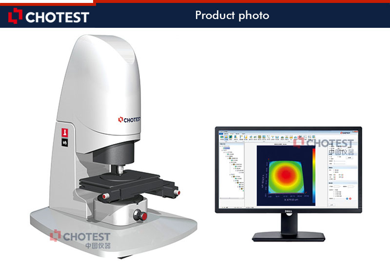
3D Optical Surface Profilometer SuperView W1

Contact Now* Send an Inquiry to this supplier.
or
Start Order * Name your price
You may also be intersted in
micro-nano level measurem

Contact us

CHOTEST Technology Inc.
[China]

Address
2/F, Building B1, Zhiyuan, Xueyuan Road, Xili, Nanshan, Shenzhen 518071, China Shenzhen Guangdong
Phone
86-83318988-227
Contact name
Omiga

Quick Information

  • Brand Name: CHOTEST
  • Place of Origin: China
  • Model Number : SuperView W1
  • :

Description

  • Model No.: SuperView W1/W1-Pro
    Product name: Nano 3D Optical Surface Profilometers
    Standard field of view: (0.98*0.98)mm
    Max field of view: (6x6)mm
    Reflectivity of test object: 0.5 % ~100 %
    Repeatability of Roughness RMS: 0.005nm
    Scanning range: ≤10mm Resolution: 0.1nm
    Accuracy of stage measurement: 0.3 %
    Repeatability of stage measurement: 0.08% 1σ

Description

SuperView W1 Optical 3D Surface profilometer is an ideal instrument for sub-Nanometer measurement of various precision parts. Based on the principle of white light interference technology, combined with precision Z-direction scanning module and 3D modeling algorithm, it contactlessly scans the surface of the object then establish a 3D image for the surface. A serial of 2D, 3D parameters  reflecting surface quality of the object are obtained after XtremeVision software processes and analyzes the 3D image.    The SuperView W1 is a user-friendly precision optical instrument with powerful analysis functions for all kinds of surface form & roughness parameters. With unique light source it could measure various precision parts with both smooth and rough surface.

Parameters

Model No. SuperView W1 SuperView W1-Pro
Light source White LED
Video system 1024×1024
Standard Field of View 0.98×0.98 mm
Max Field of View 6.0×6.0 mm(Optional)
Lens Turret Manual 3 holes turret(Optional: Motaorized 5 holes turret)
XY Object table Size 320×200mm 300×300mm
Moving range 140×100mm 200×200mm
Loading capacity 10kg
Control method Motorized
Tilt ±5°
Z Axis  Tracvel range 100mm
Control method Motorized
Z Stroke Scanning range 10mm
Surface Form Repeaability*2 0.1nm
Roughness RMS Repeatability*3 0.005nm
Step Hiehgt Measurementy*4 Accuracy: 0.3% Repeatability: 0.008%(1σ)
Scanning Speed at 0.1nm resulution 1.85μm/s
Reflectivity of Test Object 0.05%~100%
Size(L*W*H) 700x606x920mm
Weight <160kg
Operating Environment Temperature 15°C~30°C, fuctuation <1°C/15min
Humidity  5%~95% RH, no condensation
Vibration VC-C or better
Software Noise Evaluation*5 3σ≤4nm
Compressed Air 0.6Mpa oil-free, water-free, 6mm diameter of hose
Power Supply AC100~240V, 50/60Hz, 4A, 300W
Other No strong magnetic field, No corrosive gas
*1 W1 is the standard model of 3D Optical Surface Profilometer; W1-pro has larger stage size and travel range. W1-Ultra has greatly improved the scanning speed compared to W1.
*2 Use EPSl mode to measure Sa 0.2nm silicon wafer in the laboratory environment; Single stripe, 80um filter for full field of view
*3 Measure Sa 0.2nm silicon wafer in a laboratory environment according to the ISO 25178.
*4 Measure standard 4.7μm steps height block in a laboratory environment according to the ISO 5436-1:2000
*5 When the software noise evaluation is 4nm≤3σ≤10nm, the Roughness RMS repeatability is revised down to 0.015nm, the Step height measurement accuracy is revised down to 0.7%, and the step height measurement repeatability is revised down to 0.12%; When the software noise evaluation is 3σ>10nm, the environment does not meet the requirement for usage of the equipment, and need to change the site.

Remark: Performance parameters are tested by using a 4.7µm precision master stage gauge in lab according to ISO 4287 and ISO 25178.

Zoom ratio of lens

2.5×

5×

10×

20×

50×

100×

Numerical hole diameter

0.075

0.13

0.3

0.4

0.55

0.7

Optical resolution at 550nm (µm )

3.7

2.1

0.92

0.69

0.5

0.4

Depth of focus( µm)

48.6

16.2

3.04

1.71

0.9

0.56

Working distance( mm)

10.3

9.3

7.4

4.7

3.4

2.0

Field H ×V

(mm)

Video system

1024×1024

0.5×

3.92× 3.92

1.96×1.96

0.98×0.98

0.49×0.49

0.196×0.196

0.098×0.0 98

0.75×

2.6× 2.6

1.3×1.3

0.65×0.65

0.325×0.325

0.13×0.13

0.065×0.065

1×

1.96× 1.96

0.98×0.98

0.49×0.49

0.245×0.245

0.098×0.098

0.049 ×0.049

※ Built-in  ISO/ASME/EUR/GBT Standards of 2D, 3D parameters: 

2D Parameters

Standard

Parameters

ISO 4287-1997


Principal section

Roughness

Waviness

Amplitude

Pp, Pv ,Pz, Pc, Pt,Pa,Pq,Psk,Pku

Rp, Rv ,Rz, Rc, Rt,Ra,Rq,Rsk,Rku

Wp, Wv ,Wz, Wc, Wt,Wa,Wq,Wsk,Wku

interval

PSm,Pdq

RSm,Rdq

WSm,Wdq

Substance

Pmr,Pdc

Rmr,Rdc,Rmr(Rz/4)

Wmr,Wdc,Wmr(Wz/4)

Peak

PPc

RPc

WPc

ISO 13565

ISO 13565-2

Rk,Rpk,Rvk,Mr1,Mr2,A1,A2,Rpk,Rvk

ISO 12085

Roughness graph

R,AR,R× ,Nr

Waviness  graph

W,AW,W×,Wte

Other graph

Rke,Rpke,Rvke

AMSE  B46.1 

2D

Rt,Rp,Rv,Rz,Rpm,Rma×,Ra,Rq,Rsk,Rku,tp,Htp,Pc,Rda,Rdq,RSm,Wt

DIN EN ISO 4287-2010

Original profile

Pa,Pq,Pp,Pv,Pz,Pc,Pt,PSk,PKu,PSm,PPc,Pdq,Pdc,Pmr,

Roughness

Ra,Rq,Rp,Rv,Rz,Rc,Rt,RSk,RKu,RSm,RPc,Rdq,Rdc,Rmr,

Waviness

Wa,Wq,Wp,Wv,Wz,Wc,Wt,WSk,WKu,WSm,WPc,Wdq,Wdc,Wmr

JIS B0601-2013

Original profile

Pa,Pq,Pp,Pv,Pz,Pc,Pt,PSk,PKu,PSm,PPc,Pdq,Pdc,Pmr,

Roughness

Ra,Rq,Rp,Rv,Rz,Rc,Rt,RSk,RKu,RSm,Rdq,Rdc,Rmr

Waviness

Wa,Wq,Wp,Wv,Wz,Wc,Wt,WSk,WKu,WSm,WPc,Wdq,Wdc,Wmr

GBT 3505-2009

Original profile

Pa,Pq,Pp,Pv,Pz,Pc,Pt,PSk,PKu,PSm,PPc,Pdq,Pdc,Pmr,

Roughness

Ra,Rq,Rp,Rv,Rz,Rc,Rt,RSk,RKu,RSm,Rdq,Rdc,Rmr

Waviness

Wa,Wq,Wp,Wv,Wz,Wc,Wt,WSk,WKu,WSm,WPc,Wdq,Wdc,Wmr

3D Parameters

Standard

Parameters

ISO 25178

Height

Sq,Ssk,Sku,Sp,Sv,Sz,Sa

function

Smr,Smc,S×p

Space

Sal,Str,Std

Composite parameters

Sdq,Sdr

Volume

Vm,Vv,Vmp,Vmc,Vvc,Vvv

Form

Spd,Spc,S10z,S5p,S5v,Sda,Sha,Sdv,Shv

Functional

Sk,Spk,Svk,Smr1,Smr2,Spq,Svq,Smq

ISO 12781

Flatness

FLTt,FLTp,FLTv,FLTq

EUR 15178N

Amplitude

Sa,Sq,Sz,Ssk,Sku,Sp,Sv,St

Space

Str,Std,Sal

Composite parameters

Sdq,Sds,Ssc,Sdr,Sfd

Area, Volume

Smr,Sdc

Function

Sk,Spk,Svk,Sr1,Sr2,Spq,Svq,Smq

Functional

Sbi,Sci,Svi

EUR 16145 EN

Amplitude

Sa,Sq,Sy,Sz,Ssk,Sku

Mixed parameters

Ssc,Sdq,Sdr

Functional

Sbi,Sci,Svi,Sk,Spk,Svk

Space

Sds,Std,Stdi,Srw,Srwi

Hardness

Hs,Hvol,Hv,Hps,Hpvol,Hpv,Hap,Hbp

ASME B46.1

3D

St,Sp,Sv,Sq,Sa,Ssk,Sku,SWt

Applications

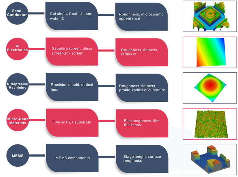
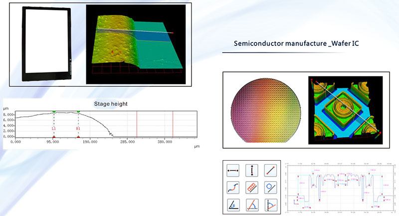
It is used for measurement and analysis of surface roughness and profile of precision components from industries of semi-conductor, 3C Electronics, ultraprecise machining, optical machining, micro-nano materials, micro-electro-mechanical system.

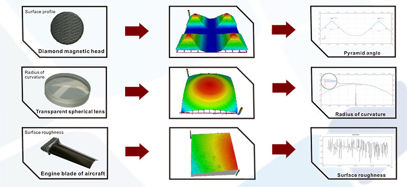
Measurement and analysis for various products, components and materials`surface form and profile characteristics, such as flatness, roughness, waviness, appearance, surface defect, abrasion,corrosion, gap, hole, stage, curvature, deformation, etc.

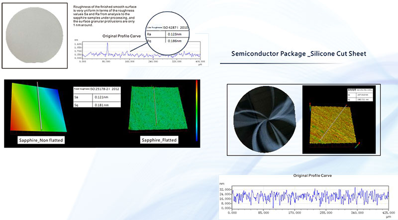
3C Electronics_Sapphire crystal

3C Electronics _ Ink screen


Packaging & Delivery

  • Delivery Lead Time : 30
  • Supply Ability : 30

Product Image

  • 3D Optical Surface Profilometer SuperView W1 image

Other products from this supplier

Related products from premium suppliers on EC21

Send an Inquiry to this supplier

Send an Inquiry to this supplier
* From
  To Omiga
CHOTEST Technology Inc.
* Buying Product
- Please enter your specific buying item.
e.g. 42 inch LCD TV, leather executive chair
Category : Other Optics Instruments
* Message

Use English only Max. 2000 characters. (Min. 20)

Send
EC21.com does not guarantee the validity of product information or the credentials of sellers.

Browse: Manufacturer Directory Premium Suppliers Site Map

About EC21 Contact Us Terms & Conditions Report Item Online Trading Risks Product Listing Policy

Copyright (c)1997-2026 EC21 Inc. All Rights Reserved. EC21 in KoreanChinese

Business Registry Number: 120-86-03931 | Mall order sales Registration Number: 강남-5838